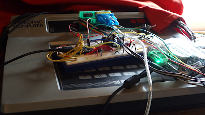
Designing the Videopac SDCart. Pt.3 Arduino and Videpac data transactions
Introduction
In the last post (Pt.2) we got a game from the sdcart transfered to the Videopac. This was done while holding the system in reset while taking over the databus. This worked but I wasn't happy with having 20 I/Os of data, address, and control going through transievers.In this part 3 we switch to having a single 8-bit buffer on the arduino that the vp can access, and let the videopac control the system bus at all time. Less bus-transceivers, allthough I need to store the menu program on ROM and not SD card.
We will look at:
- Bustransciever and control
- bus activity
- Find I/O on the cart port for serial tx
Prototyping
I'm using Sören Gust's ramcart, the aswcurr assembler and sometimes the o2em emulator. My design is partly based on the ramcart (menu rom and game in ram). |
| Prototyping: Videopac, Arduino nano, 74LS245, 74LS00, and Digilent Digital Discovery 2. |
The atmega328p and the bustransceiver:
Serial TX I/O on the cartport (A13)
There is no such thing. I needed a tx pin to send requests to the arduino, like card-inserted, directory listing or read rom image. The I/O is bitbanged in a timed manner. At first I tried using the CS pin. It kinda worked, but interrupts made it change state. I need the IO to be clean for the whole durration of the menu program. We need interrupts also.How about A13 ? What ? Address bus as TX ?? A13 is part of banking, but it also a writeable I/O on port P1. The program crashed! Bummer, well not really. While game roms might use it, the program rom doesn't have to. So I cut a trace on the ramcart and tied ROM_A13 to a power rail, and no more crash! In the schematic above I have A13 connected to the arduino. I'm using software serial to receive one byte commands from the videopac.
The data response and control lines
In the schematic it has a nand gate that produce OE_N = RD * CS, but the image below show that RD and CS is not enough. System crash follows. |
| Unwanted outputenable (DIN7), probably from vdc interrupts |
The arduino receives a command and responds with data. You can see that to the right in illustration above (din0-3). I'm only looking at four bits for the moment. DIN7 is the outputenable and was always high, so the data was not received from the buffer transceiver.
RD, CS and #OE_from_avr now fixes this problem. It blocks out those unwanted reads. Firs tyou see the serial command h01 from the videopac on the top. Then the CS_from_arduino and CS passes RD to the transceiver. You can see a quick burst of reads right before the arduino databus goes from ff (stop) to 00 (start). Once the videopac receives a zero, it starts counting 1.5 cycles to hit the middle of the first byte to read. Here the assembly routines hasn't been tweeked to perfection yet.
Result after sending 01 to the atmega and receiving 0-9 as data:
There you go. Woops, why are the numbers received in the wrong order? Or are they
Gotcha, had pin 0-2 reversed on the breadboard :D
What's next ?
Next we want to get sdcard content listing on the screen. Easier said than done.The videopac con only hold a line of text, some "quads" and four sprites. We need to do some handsome irq dancing and timer ticking to update this goldfish memory of a videopac register to get multiple lines. Not sure how to do it yet, but from what I've seen is that we set the vdc chip to interrupt on horizontal lines, set the timer to count until we are at the right spot, turn off graphics, update the line, turn the graphics back on... Tricky..
Peek in my code if you like at this github commit (theversion at the time of this writing).
commit fe73cc9a
Related video:


Kommentarer
Legg inn en kommentar