Designing the Videopac SDCart. 2: The SD Cart demo
Introduction
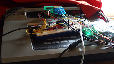
I managed to get several ROM binaries on an SD card to interface and run on the Videopac G7000. Last weekend I made a video about the progress so far.It was not all easy. The damn roms wouldn't run from the SRAM. Some problems were ironed out, but remaining was the problem of which address lines to use. The buses were isolated with three 8-bit transcievers, but two of them might be replaced by resistors. Sören Gust's gold mine recide in the archive.org. It was complete with design files for the G7000 RAM cart where you can connect a PC and transfer a ROM via serial. He also shared his source code and documents on the bios library.
The Program Memory Map
Often address line A10 is not used in game carts. Lets have a look at the memory map.In the program memory map for the Intel 8048, the first 1kb is reserved for the internal program memory, and the remaining 3kb is external program memory. These are accessed with A11..A0. Port1 pins P0 and P1 can be used for banking, and are routed to the cartridge port. Note that these are not associated with the program-counter, and bank selecting is done manually in software. Therefore the 1kb internal repeats in every bank. It is possible to have 3kb, 6kb, 9kb or 12kb external memory with P0 and P1.

Mirroring of data in a memory map will happen whenever an address line is not connected. Consider that if a 2kb ROM was attached to A10 down to A0. Half of the ROM is waisted by the internal memory..Now remove A10 and hook up A11 instead, and the 2kb of data will be mirrored to cover 4kb of memory space. The MCU can now access the full 2k of data.
The assembly code has to have its origin at $0400, even though on the ROM the data is located at $0000.
Multiplexing or 1:1
Lets asume we are designing the SD Cart PCB. We want to load a binary from SD card into SRAM. If we use multiplexing or signal exchangers we can get away with less data loaded into the SRAM. Instead we can connect the SRAM 1:1 with the Address bus. 1:1 is the most flexible solution. Now we can have all the memory available to the VideopacIf we load a 2kb cart rom who is not using A10 then we must ensure the data is mirrored. Another issue, lets say we use a 16kb SRAM for the four banks (See P0 and P1 above), then when the computer restarts, we don't know which bank it starts in. I've read that it often starts in bank 3. So data must be mirrored to all banks. It gets a bit hairy, so lets repeat:
2kb ROM mirrored to 4kb in the first bank. Copy the first bank into the remaining banks.
Ideas for a menu system.
Entering the menu
The cartridge port does not have a reset pin. To listen for a reset we can monitor P0 and P1 and perhaps also other I/O. They should all go HIGH. Rene's flash cart enters the menu program after holding reset for more than three seconds.You can't really write to the program memory (the SRAM in our case) asynchronously while the cpu is currently accessing code from it. An idea is to load the menu code from SD into SRAM while the user is holding the RESET button. At the same time, a list of contents on the SD can be written to SRAM for the menu program to read.
Select Game
RAM for both Menu and Game
When the user finds a game to load and press the fire button, how is the game loaded into RAM? As mentioned above, we can't write to RAM if the menu is running on it. Shall we listen for a RESET? Another way is perhaps to jump to the bios routine select-game. Now the CPU is running in the internal program memory, and the select-game routine is waiting for the user to hit a key. The external bus is therefore free, and the MCU can write to RAM. When the user hits a number on the keyboard, the bios jumps back to a start-game address on our freshly re-written RAM. The reason why I like this scheme is because it eliminates the need for a ROM.
In the select-game routine, the CPU polls the keyboard matrix. The CPU borrows Port2 which is also connected to the cartridges A8..A11. These high-address lines must be buffered to not crash with the MCU's programming of the RAM!
 |
| The keyboard scanner and A8..A11 share I/O on Port2. |
RAM + ROM
With separate RAM and ROM, the Menu can be permanently stored in ROM and is ready at power-up. As we can see in Sören Gust's G7000RAM Cart, the control signals can be multiplexed with the RAM and ROM. In Menu mode, the RAM is write-only. The G7000RAM Cart works in that way that data enters serially through the T0 pin, and every byte received is written to the RAM immediately. When transfer is complete, the user flips the switch and hits the reset and the game starts. A similar scheme can be done with the SD Cart, but with parallel transfer instead.
In our case, if we had a separate RAM + ROM, the MCU can program the RAM while the code is running in ROM and then jump to select game or the reset routines.
Another way of getting data into RAM is (as mentioned earlier) to let the CPU fetch data from a latch and write it to RAM. The MCU and the CPU must handshake. Why is this interesting ? If the MCU writes to RAM we need buffers and the buffers has to be turned off to separate the RAM from the B and Address busses. If we instead hook a latch up to the databus, and hook its output-enable to /RD, then a read issued by the CPU will fetch the latch's content, and the cpu will write it to RAM at the correct address without the need for a horde of 74LS245s, and also no need for address lines to the MCU!
What is the best. RAM + ROM and less buss transcievers/buffers, or the single ram holding Menu and game written to at the hold of reset and while the code is running in the internal select game routine? Having the CPU do the handshaking and writing to MCU will require more advanced coding. But has that ever stopped anyone ?

Another way to detect reset is to see if there is a /PSEN with only A10 set. The first command post reset is a JMP to 0400 (which is the first external program address).
SvarSlettNot sure if the /PSEN and address bus is used when the 8048 is running the internal 1K ROM. I have to hook up a logic analyzer or an arduino, and check.
Another way could be to use the T0 input on the processor as a signal that shows the RAM is loaded. In the file selection program you just check if T0 is set, and if so, do a
MOV A,#00
MOV PSW,A
JMP 000
This should reset the stack point and reset the Odyssey, without having to press the reset button.