Designing the Videopac SDCart. 1: The MCU and system bus.
Introduction
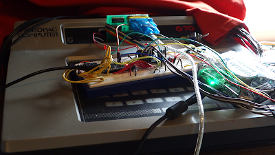
We will look at the Videopac's digitial system. It is a cartridge based gaming console. The intention of these blog series is to design an SDcard interface. First I'd like to get to know the system, and I will be focusing on the signals present at the Cartridge port.System specs
- CPU: Intel 8048 8-bit @ 1,79 MHz
- Memory:
- RAM: 64 bytes
- AV-RAM: 128 bytes
- BIOS-ROM: 1k bytes
- Cartridges: 2k, 4k and 8k bytes
The Intel 8048 microcontroller
The videopac has a MCU with- 1k bytes of BIOS ROM.
- 27 I/O
- 8-bit timer/counter
- Onboard oscillator/clock circuits
- Address latch enable (ALE)
- 96 instructions, 1 and 2 bytes long.
The digital design of the Videopac
The 8048 MCU has an internal rom preprogrammed with a bios. The video/audio chip is the Intel 8244 (NTSC) or 8245 (PAL) custom IC with 128 bytes of memoryThe keyboard is scanned using decoders and encoder ICs hooked up to the MCU I/Os. Some of these I/Os are shared with the banking (A8...A11) of the Cartridge ROM memory. The joysticks are fed through two buffers on the BUS. The buffers are controlled by the keyboard matrix decoders and a MCU I/O.
The ROM cartridges can be 2k, 4k and 8k. In the schematics I can only see A11..A0. That is not enough memory space to access 8k.
The System BUS
The mainboard has a BUS {B7..B0} transfering address and data to or from the address latch, RAM, video/audio IC, cartridge ROM, and joystick buffers.From the Intel 8048 DB0-DB7 BUS datasheet: "True bidirectional port which can be written or read synchronously using /RD and /WR strobes. The port can also be statically latched. Contains the 8 low order program counter bits during an external program memory fetch, and receives the addressed instruction under the control of /PSEN. Also contains the address and data during an external RAM data store instruction, under control of ALE, /RD and /WR."
The control bus is driven by the MCUs I/O, ALE, /PSEN (cartridge rom strobe), /RD and WR (memory/peripherial ic read and write strobes), and are mixed with OR and NAND gates to form chipselects, read and write strobes for RAM, ROM and the VIDEO IC. Unlike systems like the C64 with a PLA to decode A12...A15 together with other signals to map in memory devices by generating chipselects based on addresses, the Videopac access only 256 bytes and MCU I/O is used instead and mixed with RD/WR. For example look at these logic expressions formed by the control bus. Note that these memory ICs have two chipselects. The datasheet names these CS and /CS, but for sanity we will call them /CS1 and CS2
- ROM_CS2 = P14 = /RAM_CS1
- /ROM_WR = P16 + /WR
- /RAM_WR = /ROM_WR
- /ROM_CS1 = /( ( /RD ) * ( /ROM_WR ) )
- RAM_CS2 = /ROM_CS1
- /VIDEO_CS1 = P3
- /VIDEO_RD = P16 + /RD
- /VIDEO_WR = /WR

The 8244/8245 VDC actually has 256 bytes of memory, and an internal character set ROM. The Videopac uses a Motorola 6810 RAM chip providing 128 bytes of additional data RAM.
SvarSlettROM cartridges usually use the 8048's A0-A9, A11 (mapped to A10 on the cart), P10 (mapped to A11 on the cart) and P11 (mapped to A12 on the cart). If the cart is 2K, obviously it doesn't use A11 or A12. Mapping A11 to A10 on the cart makes 000 in cartridge space appear as 400h to the processor. On power up, P10 and P11 = 1. Exceptions to this mapping are Videopac 31, 40 and "Kill the Attacking Aliens".
There's a slash missing before "WR", which is also an inverted signal.
P13 is used as /VDC_CS.
P14 is used as /RAM_CS, and available on the expansion port. It's not used for ROM_CS.
P16 is used to quickly copy data from RAM to the VDC (a MOVX A,@Rr reads from RAM and MOVX @Rr,A writes to the VDC). P13 and P14 also have to be low for this to work.